Electronics Publications
High-resolution nondestructive 3D imaging
Bruce Johnson
Chip Scale Review, November/December 2013, 24-27
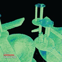
Applying x-ray microscopy and finite element modeling to identify the mechanism of stress-assisted void growth in through-silicon vias
L.W. Kong, J.R. Lloyd, K.B. Yeap, E. Zschech, et al.
J. Appl. Phys. 110, 053502 (2011)
DOI : 10.1063/1.3629988, finite element analysis, silicon, stress effects, three-dimensional integrated circuits
Metrology and Failure Analysis for 3D IC Integration
E. Zschech, A. Diebold
AIP Conf. Proc. 1395, 233-239 (2011)
DOI: 10.1063/1.3657897, metrology, failure analysis, three-dimensional integrated circuits, TSV
X-ray computed tomography for non-destructive failure analysis in microelectronics
M. Pacheco, D. Goyal
Reliability Physics Symposium (IRPS), 2010 IEEE International 252-258 (2010)
DOI: 10.1109/IRPS.2010.5488820, failure analysis, Thermal Stress, Solder Bump Cracking
Deposition processes for competitive through silicon via interposer for 3D
C. Uzoh, R. Sharna, P. Monajemi, M. Newman, et al.
Paper presented at IWLPC 2012, San Jose, CA
Read paper here, TSV, cavity fill efficiency, plating planarization factor
High-resolution X-ray imaging - a powerful nondestructive technique for applications in semiconductor industry
E. Zschech, W. Yun, G. Schneider
Appl. Phys. A 92, 423-429 (2008)
DOI: 10.1007/s00339-008-4551-x, failure analysis, in situ, interconnect degradation